power factor correction
Power factor correction is needed because of ill-conditioned current wave forms. Generally the voltage is a sinusoid from the AC mains. The current the load draws may be far from sinusoidal, having higher order harmonics than the fundamental. This phenomenon causes inefficiencies in the power delivery system since the generator and transformers were not designed to handle higher harmonic components Power factor correction works by making the load look resistive, that is to say, so that the current in the load is exactly proportional to the voltage supplied. For many modern loads, like power supplies and LED lighting, this may be a problem which needs to be addressed in designing the power supply for these loads.
|
|
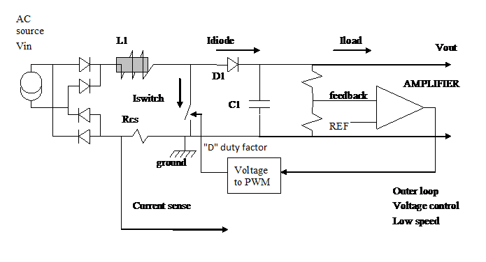
Power supplies which convert from AC to DC are usually switchmode supplies. The first stage of regulation converts the AC to a high voltage intermediate DC voltage. The basic circuit to do this looks like the schematic on the left. An amplifier compares the output voltage to a reference and feeds the error back to a Voltage to PWM converter which puts out pulses at a constant frequency with the duty factor, D, or the switch on-time modulated by the error voltage The nice feature about this circuit is that it is inherently power factor corrected as long as the output voltage is high and as long as the load current is moderate.
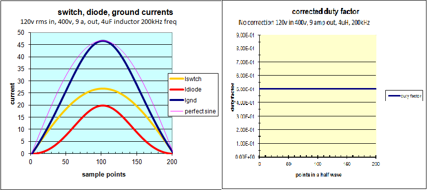
This feature can be seen in the plot on the right. This is the result of the uncompensated above circuit run at a moderate current with a relative high output voltage. The average currents are plotted as a function of time on the X axis. The light pink line is a perfect sine wave The blue line is the actual ground current of the circuit is this configuration. The power factor is OK, not wonderful but nearly correct. The actual conditions are Vin=120 vrms, Iout=9 amperes, Lind=4uH, Fpwm=200kHz.. The output power is 3600 watts.
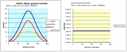
However, if the output voltage is decreased the power factor can be come rather poorer as shown in the next plot. This plot was made with the same conditions as above except for Vout=250 volts. The better power factor in the higher voltage case is a result of the fact fact that, on each cycle, the current in the inductor goes to zero faster while the inductor is discharging into a higher voltage. One of the most common ways of effecting power factor correction is to force the current curve into a sine wave. This is normally done by multiplying the voltage error signal by a sine wave derived from the input rectified AC mains. The product signal is then applied to a circuit which is self oscillating. When the current in the inductor falls to zero, the power switch is turned on. The power switch is turned off when the current in the switch exceeds the product feedback signal on a cycle by cycle basis. There are several disadvantages to this method. At low current, at the tails of the sine wave, the frequency increases in order to create the sine wave replica. The result is a non-constant switching frequency with some very fast switching in the lower current ends. The switch current sense has to be a fast loop, operating on a cycle by cycle basis in a very noisy signal environment with lots of ringing, spikes, and capacitive coupling. |
|
|
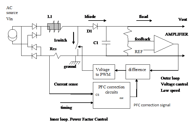
The invention here is to eliminate the need for the fast current sense and feedback and to take advantage of all the nice features of the PWM regulator mode. In order to use the PWM loop, with all of its advantages, in a well conditioned power factor mode, an addition must be made. The addition is an additive signal to the normal pulse width control from the voltage loop. This signal corrects the pulse width modulation to correct the power factor. The block diagram is shown, to the left.
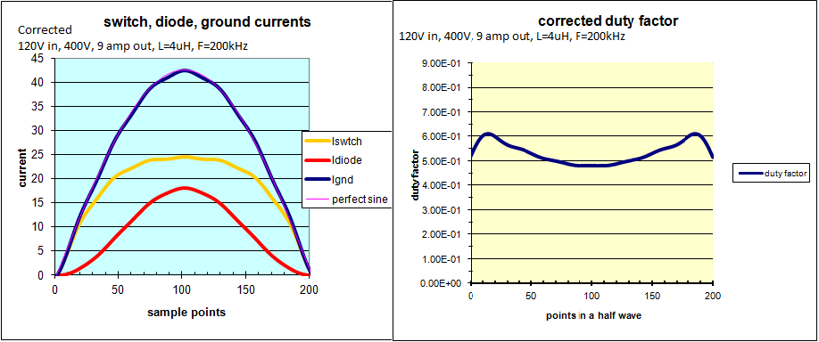
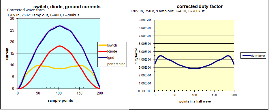
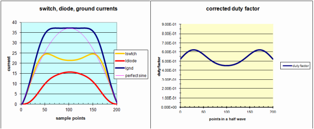
This solution works by taking a Fourier transform of the input current wave form, detecting the spurious harmonics, and then removing them with closed loop feedback. In the typical AC-DC converter, the AC wave is rectified and applied to at boost mode switching regulator. Both the rectification process and the boost mode regulation can cause distortions in the current wave form, adding higher harmonics to the current wave form. The Fourier transform operates in the time frame of the AC wave form. Current data is collected over at least one of the half wave rectified voltage waves, and at the end of the half cycle, a Fourier transform is made. The fundamental frequency is removed, leaving only the spurious harmonic content. This measurement can be band limited to a few kilohertz such that all of the switching noise is removed. This Fourier transfomed signal can even be averaged over a few cycles, improving its signal to noise. The harmonic content is then transformed back into the time domain and applied as a correction to the voltage feedback signal. Because the power factor signal is, effectively, a second order correction on the main voltage loop, the result is a power factor corrected power supply which is adaptive over an extremely wide range of input and output conditions and component variation. The PFC correction circuit might be envisioned as a small block of digital circuitry, possibly an 8 or 16 bit core with a small amount of memory. This might even be a stand-alone circuit interfacing with the PWM engine. It also could be easily integrated with a digital power control chip. The resulting circuit can then use substantially higher switching frequencies with the attendant size component value and physical size reduction, particularly the inductors. The entire loop is simplified. It is even possible to do things like make a buck/boost circuit with an output voltage lower than the input voltage utilizing the duty factor correction to effect PFC. Two main improvements can be realized using a simplified PWM converter. The first is a higher PWM frequency because current feedback is no longer cycle by cycle. The second major advantage, due to the increased switching speed, is the reduced size of the inductor or transformer energy storage element. Another fallout is that the power factor correction is improved at low current. Finally, nonlinearities in the capacitors and inductors can be accounted for. Another advantage is the ability to lower the output voltage, possibly even making the output voltage lower than the input voltage using a buck/boost converter. . These plots are examples of the operation of the harmonic removal method. In this plot the algorithm has been applied to the first example plot above. Even though the power factor of the first example was very good, the power factor of the corrected circuit is excellent, being almost a perfect sine wave. The duty cycle variation is, indeed, a second order correction on the main voltage loop. Compare with Figure 2. The second example, with the lower output voltage, but the same load current, has a somewhat worse power factor. When the algorithm is applied, again, the resultant current wave form is nearly indistinguishable from the sine wave. Compare with Figure 3. The technique offers other interesting possibilities. If the mains are tolerant of accommodating some high frequency components, it is possible to reduce the peak current by spreading out the current wave to make it a little more like a square wave, as in this example It can be seen that the switch current has been reduced by about 20% by squaring up the ground current wave form. This wave form was accomplished by adjusting the 1st and 3rd harmonics. This is the opposite of the power factor correction. If the generator is capable of supplying the higher frequency, this technique actually improves the power delivery of the generator while keeping the output current below maximum rating by about 20% as compared to Figures 2 and 4. |
Advantages:for using the Fourier harmonic detection and removal system:
Constant frequency operation
No fast current loop
Allows the switching regulator to operate at a higher frequency as a result
High frequency PWM is a simpler design
High frequency switching allows component size and cost reduction
Closed loop Power Factor Correction over a wide range of operation, temperature, input and output voltage
Flexibility in choosing the "super PFC" option of a more square input current wave form
May be adapted to a buck/boost configuration for even lower output voltgaes
May be adapted to three phase conversion and phase balancing
My patent portfolio
This is a partial list of my patents. There are still three which are pending, one of which concerns itself with power factor correction. The patents which are concerned with PFC are 3, 4, 7, and 8. and I am the owner of these patents. The pending PFC patent extends the idea by purposely making the current wave form into a more square wave. This has the effect of drawing a greater power from the generator without violating the generator’s current limit. Number 7 on this list is an expansion of number 8. Number 3 allows the PFC circuit to make a secondary voltage less than the peak voltage of the AC sine wave while creating a well conditioned current.
3 8,619,442 Boost-buck power factor correction
4 8,542,503 Systems and methods for high speed power factor correction
7 8,018,744 Power factor correction by measurement and removal of overtones
8 7,719,862 Power factor correction by measurement and removal of overtones
The final PFC patent is concerned with reducing the peak current by squaring up the current wave form utilizing the PWM mode and overtone manipulation.
The full list is below, except for the three ongoing applications. The other (not 3, 4, 7, or 8) patents on this list are assigned to the various companies I have worked for.
PAT. NO. Title
1 8,896,281 Method for generating an internal compensation network of a pole and two zeros to compensate high frequency voltage mode switching regulators
2 8,803,494 Method for reducing body diode conduction in NMOS synchronous rectifiers
3 8,619,442 Boost-buck power factor correction
4 8,542,503 Systems and methods for high speed power factor correction
5 8,482,270 Reverse current comparator for switching regulators
6 8,354,831 Reverse current comparator circuit and method for switching regulators
7 8,018,744 Power factor correction by measurement and removal of overtones
8 7,719,862 Power factor correction by measurement and removal of overtones
9 6,809,560 Load sensing circuit for a power MOSFET switch
10 6,737,841 Amplifier circuit for adding a laplace transform zero in a linear integrated circuit
11 6,724,257 Error amplifier circuit
12 6,424,132 Adding a laplace transform zero to a linear integrated circuit for frequency stability
13 6,395,591 Selective substrate implant process for decoupling analog and digital grounds
14 6,307,409 Gate driver circuit for high and low side switches with primary and secondary shoot-through protection
15 6,304,067 Adding a laplace transform zero to a linear integrated circuit for frequency stability
16 6,005,378 Compact low dropout voltage regulator using enhancement and depletion mode MOS transistors
17 6,002,244 Temperature monitoring circuit with thermal hysteresis
18 5,929,615 Step-up/step-down voltage regulator using an MOS synchronous rectifier
19 5,889,393 Voltage regulator having error and transconductance amplifiers to define multiple poles
20 5,877,534 Method of forming electrostatic discharge protection device for integrated circuit
21 5,867,014 Current sense circuit having multiple pilot and reference transistors
22 5,677,205 Method for forming electrostatic discharge protection device for integrated circuit
23 5,654,574 Electrostatic discharge protection device for integrated circuit
24 5,596,265 Band gap voltage compensation circuit
25 5,559,424 Voltage regulator having improved stability
26 5,545,909 Electrostatic discharge protection device for integrated circuit
27 5,506,496 Output control circuit for a voltage regulator
28 5,164,802 Power VDMOSFET with schottky on lightly doped drain of lateral driver FET
29 4,820,968 Compensated current sensing circuit
30 4,795,716 Method of making a power IC structure with enhancement and/or CMOS logic
31 4,725,912 Power MOS loss of ground protection
32 4,701,883 ECL/CMOS memory cell with separate read and write bit lines
33 4,701,718 CMOS high gain amplifier utilizing positive feedback
34 4,605,891 Safe operating area circuit and method for an output switching device
35 4,553,084 Current sensing circuit
36 4,453,095 ECL MOS Buffer circuits
37 4,380,706 Voltage reference circuit
38 4,319,181 Solid state current sensing circuit
39 4,231,332 Spark and dwell ignition control system using digital circuitry
3 8,619,442 Boost-buck power factor correction
4 8,542,503 Systems and methods for high speed power factor correction
7 8,018,744 Power factor correction by measurement and removal of overtones
8 7,719,862 Power factor correction by measurement and removal of overtones
The final PFC patent is concerned with reducing the peak current by squaring up the current wave form utilizing the PWM mode and overtone manipulation.
The full list is below, except for the three ongoing applications. The other (not 3, 4, 7, or 8) patents on this list are assigned to the various companies I have worked for.
PAT. NO. Title
1 8,896,281 Method for generating an internal compensation network of a pole and two zeros to compensate high frequency voltage mode switching regulators
2 8,803,494 Method for reducing body diode conduction in NMOS synchronous rectifiers
3 8,619,442 Boost-buck power factor correction
4 8,542,503 Systems and methods for high speed power factor correction
5 8,482,270 Reverse current comparator for switching regulators
6 8,354,831 Reverse current comparator circuit and method for switching regulators
7 8,018,744 Power factor correction by measurement and removal of overtones
8 7,719,862 Power factor correction by measurement and removal of overtones
9 6,809,560 Load sensing circuit for a power MOSFET switch
10 6,737,841 Amplifier circuit for adding a laplace transform zero in a linear integrated circuit
11 6,724,257 Error amplifier circuit
12 6,424,132 Adding a laplace transform zero to a linear integrated circuit for frequency stability
13 6,395,591 Selective substrate implant process for decoupling analog and digital grounds
14 6,307,409 Gate driver circuit for high and low side switches with primary and secondary shoot-through protection
15 6,304,067 Adding a laplace transform zero to a linear integrated circuit for frequency stability
16 6,005,378 Compact low dropout voltage regulator using enhancement and depletion mode MOS transistors
17 6,002,244 Temperature monitoring circuit with thermal hysteresis
18 5,929,615 Step-up/step-down voltage regulator using an MOS synchronous rectifier
19 5,889,393 Voltage regulator having error and transconductance amplifiers to define multiple poles
20 5,877,534 Method of forming electrostatic discharge protection device for integrated circuit
21 5,867,014 Current sense circuit having multiple pilot and reference transistors
22 5,677,205 Method for forming electrostatic discharge protection device for integrated circuit
23 5,654,574 Electrostatic discharge protection device for integrated circuit
24 5,596,265 Band gap voltage compensation circuit
25 5,559,424 Voltage regulator having improved stability
26 5,545,909 Electrostatic discharge protection device for integrated circuit
27 5,506,496 Output control circuit for a voltage regulator
28 5,164,802 Power VDMOSFET with schottky on lightly doped drain of lateral driver FET
29 4,820,968 Compensated current sensing circuit
30 4,795,716 Method of making a power IC structure with enhancement and/or CMOS logic
31 4,725,912 Power MOS loss of ground protection
32 4,701,883 ECL/CMOS memory cell with separate read and write bit lines
33 4,701,718 CMOS high gain amplifier utilizing positive feedback
34 4,605,891 Safe operating area circuit and method for an output switching device
35 4,553,084 Current sensing circuit
36 4,453,095 ECL MOS Buffer circuits
37 4,380,706 Voltage reference circuit
38 4,319,181 Solid state current sensing circuit
39 4,231,332 Spark and dwell ignition control system using digital circuitry
